Projects
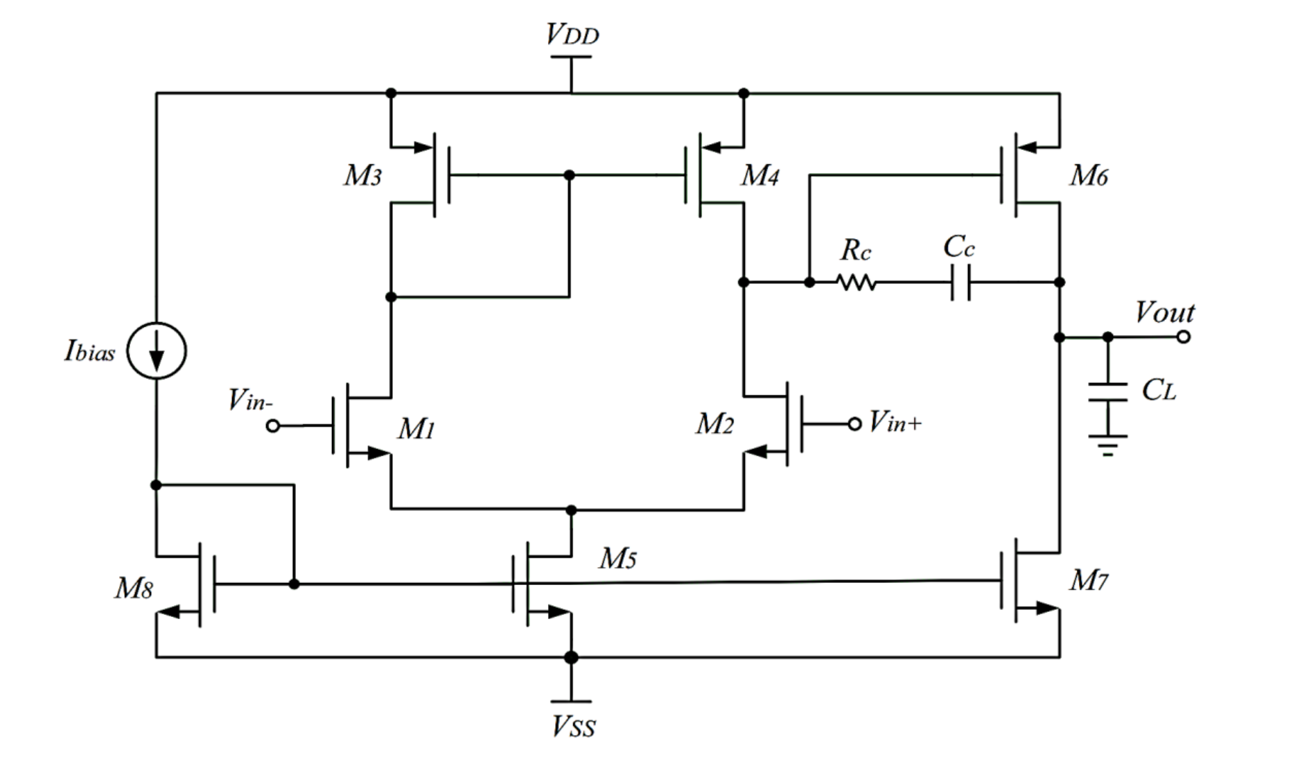
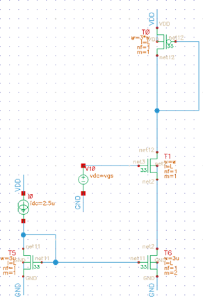
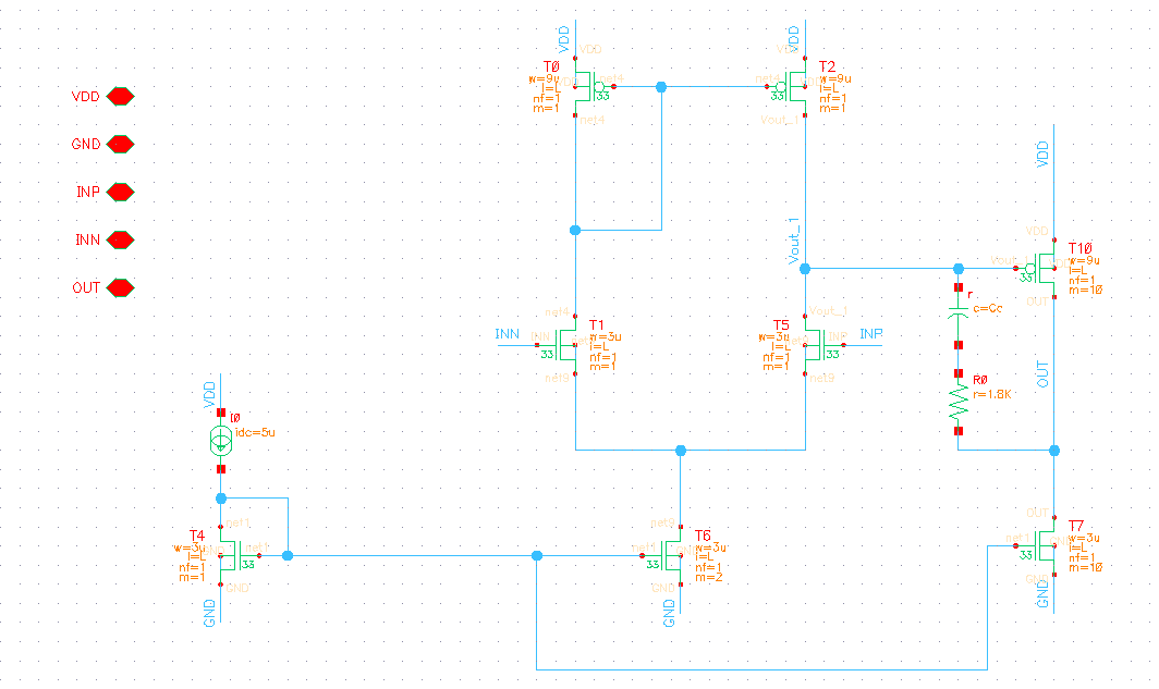
Two-Stage Miller-Compensated CMOS Op-Amp (IBM 130 nm)
Single-supply two-stage operational amplifier designed to meet stringent gain, bandwidth, stability, and power constraints using analytical small-signal modeling and transistor-level design.
- Designed a classical two-stage Miller-compensated CMOS operational amplifier using 0.13 µm CMOS technology
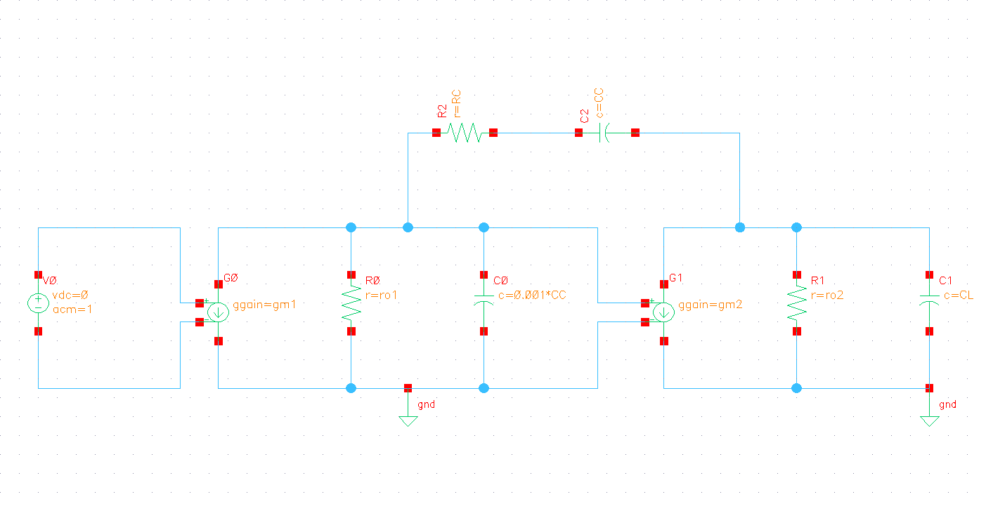
- Performed detailed small-signal analysis to determine transconductance, output resistance, gain, and frequency response
- Achieved ≥ 70 dB differential gain, ≥ 5 MHz unity-gain bandwidth, and ≥ 60° phase margin under a 2 pF load
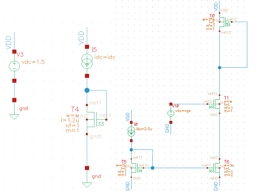
- Sized devices to satisfy ≥ 4 V/µs average slew rate and ≥ 1.2 V output swing using a single 1.5 V supply
- Met strict power and topology constraints including ≤ 0.1 mW total power dissipation and only one ideal current source
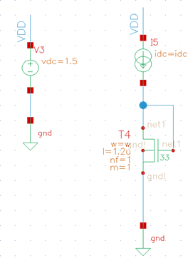
- Verified open-loop gain, phase margin, slew rate, output swing, and CMRR using Cadence ADE simulations
Synchronous Half-Bridge Buck Converter (TSMC 180 nm HV BCD)
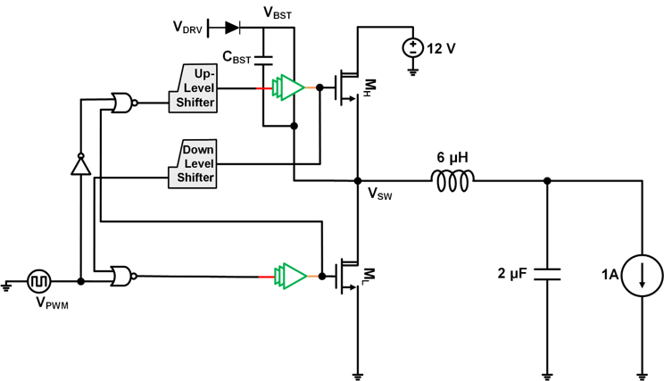
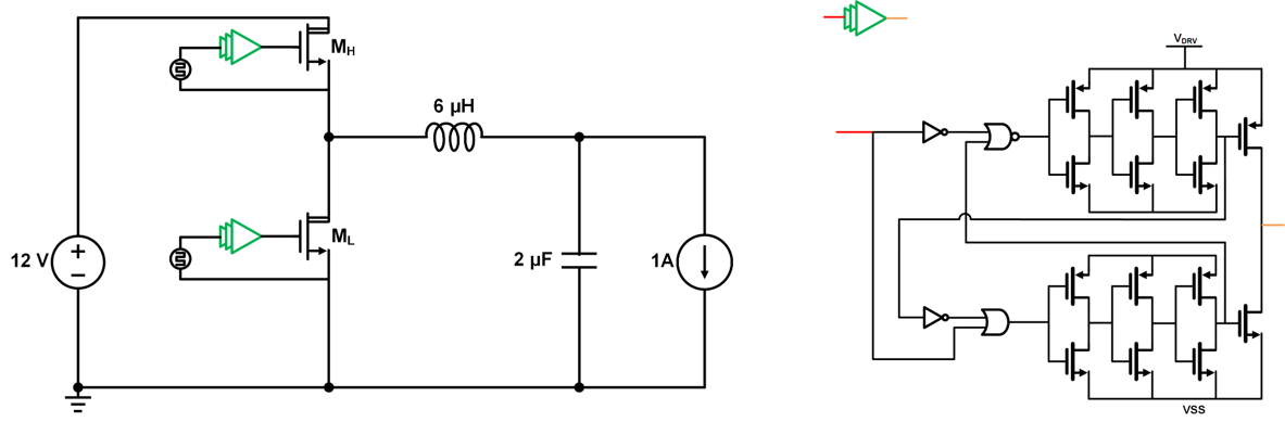
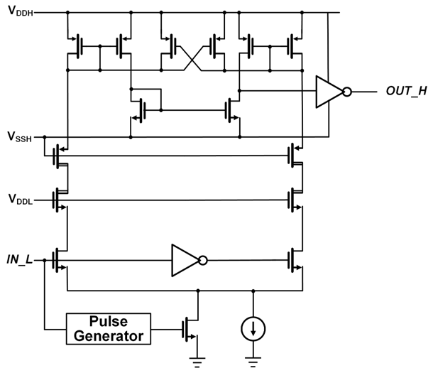
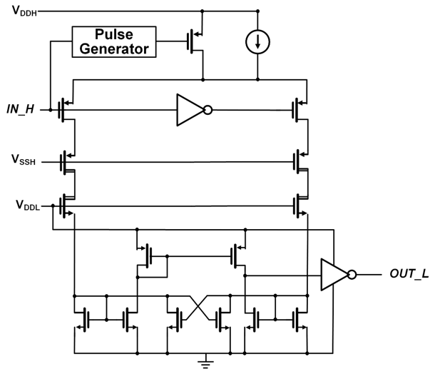
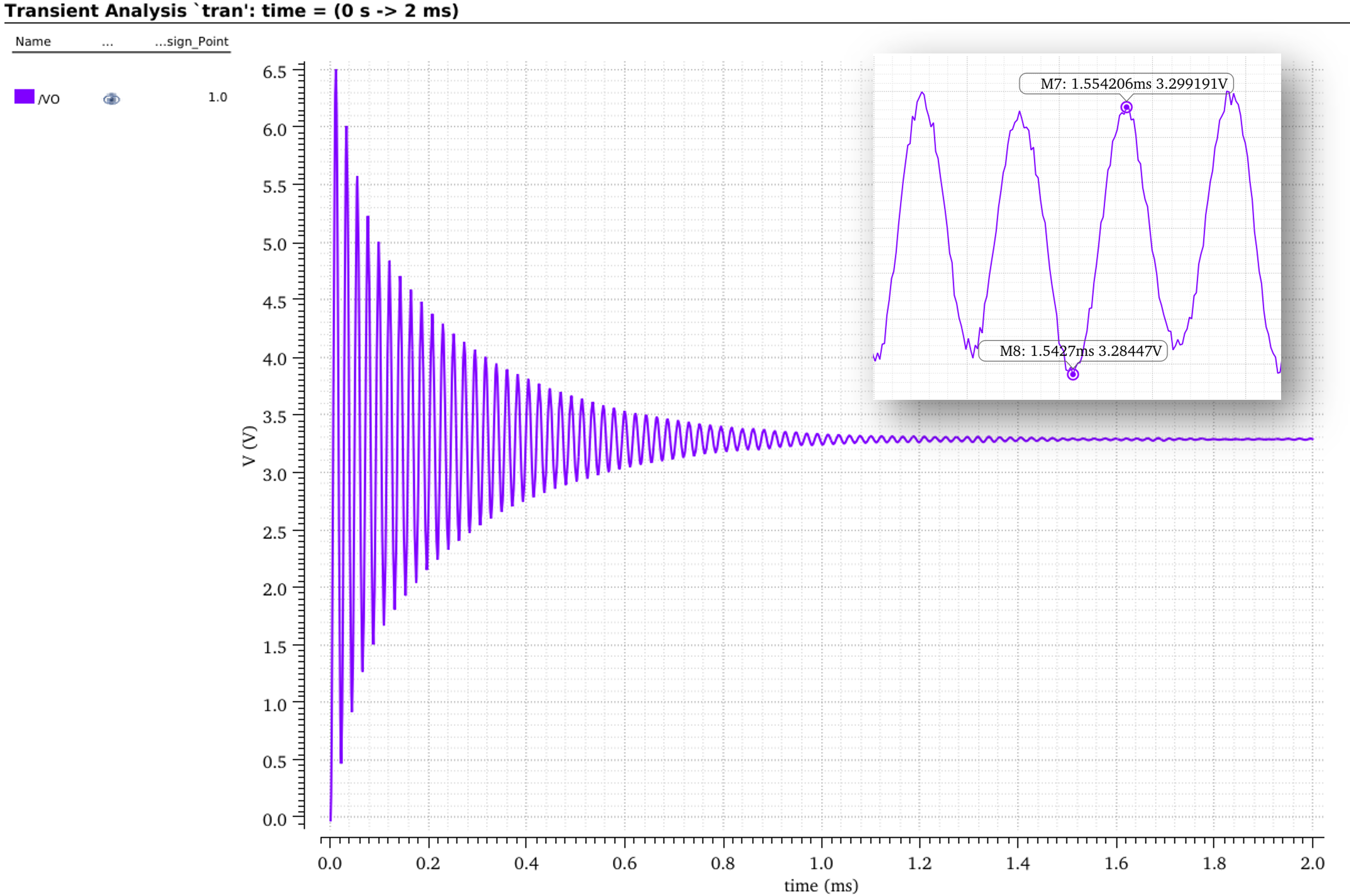
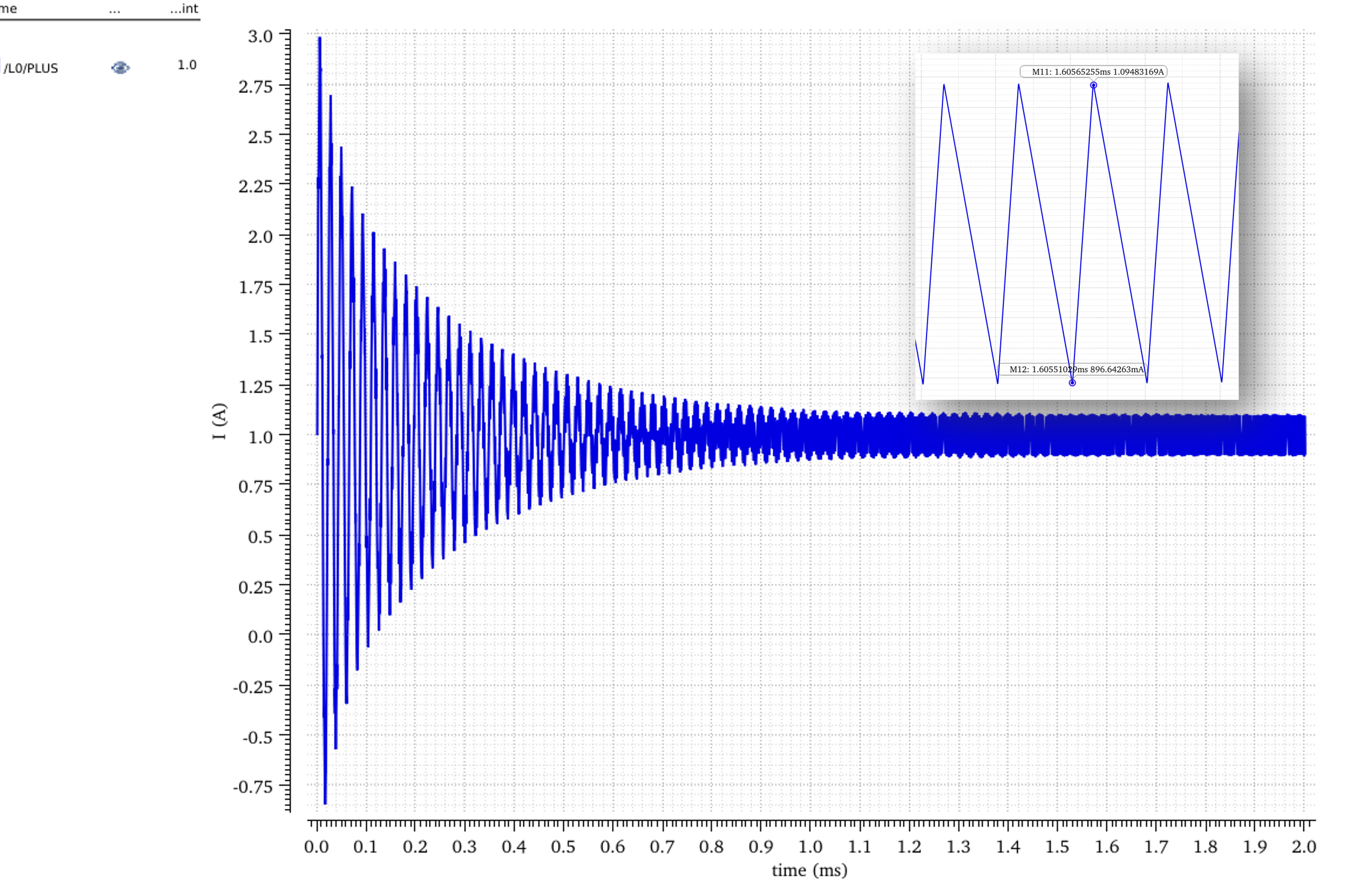
12 V → 3.3 V, 1 A, 2 MHz synchronous DC-DC buck converter with on-chip gate-driver chain (level shifters + dead-time + bootstrap), validated in Cadence Spectre.
- Designed a 12 V-to-3.3 V, 1 A, 2 MHz buck converter power stage with LC output filtering
- Analyzed key challenges: switching/conduction losses, component selection (inductor/capacitor), and ripple constraints
- Implemented full gate-driver system: up-level shifter, down-level shifter, dead-time control, and bootstrap circuit
- Set final driver-stage sizing to achieve ~5 ns rise (high-side), ~2 ns rise (low-side), and ~1 ns fall times; logic gating prevents shoot-through
- Optimized MOSFET widths via efficiency sweeps; best total widths: 65.6 mm (high-side) and 96.4 mm (low-side), with L = 900 nm
- Verified waveforms: PWM input, HS/LS VGS, level-shifter I/O, bootstrap voltage; measured ~5.15% Vout ripple and ~198 mA inductor ripple
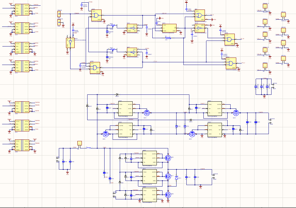
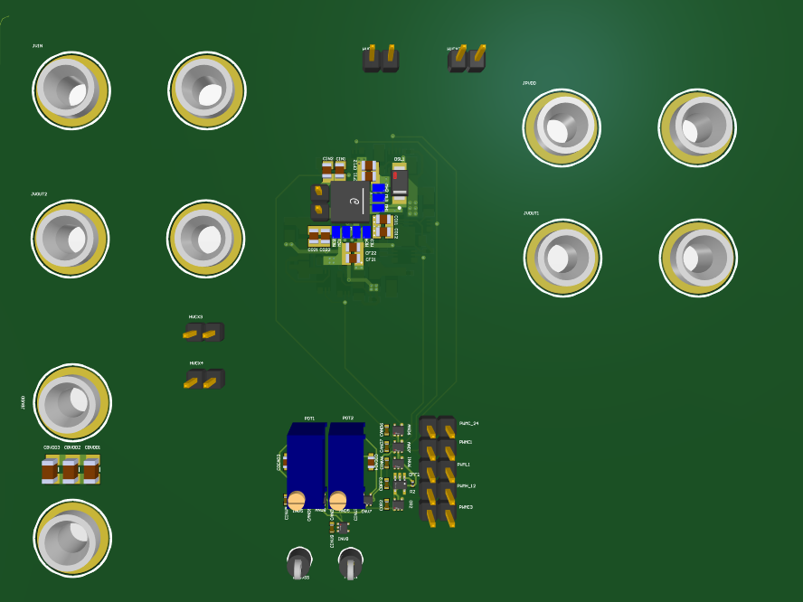
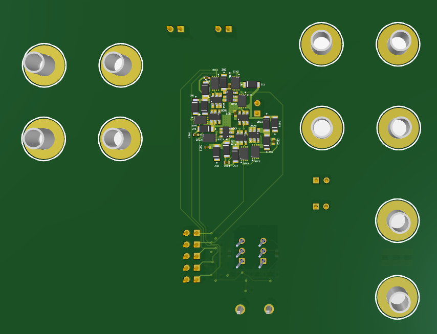
Four-Layer Power Converter PCB (Altium Designer)
Four-layer PCB prototype for a compact dual-rail power delivery concept targeting efficient silicon-to-wide-bandgap interface rails.
- Developed a complete schematic-to-layout workflow in Altium Designer for a research prototype power board
- Applied EMI-aware stackup and routing practices to support high-frequency switching and clean return paths
- Designed top and bottom signal/power routing with dedicated internal reference planes for improved signal integrity
- Prepared manufacturing outputs (Gerbers/drill files) and documentation for prototype fabrication and testing
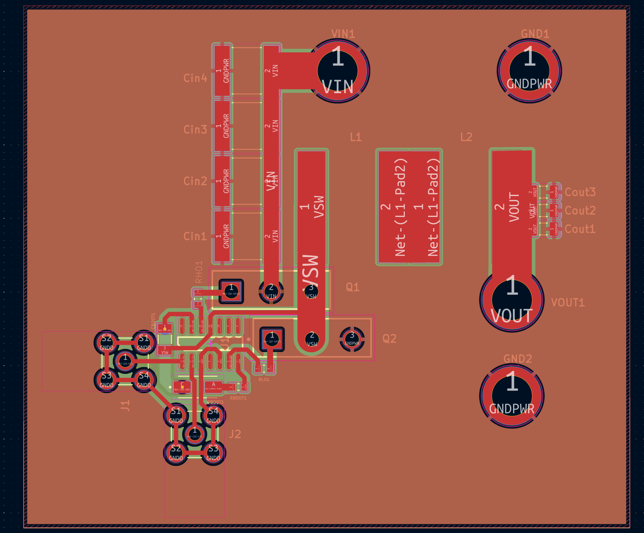
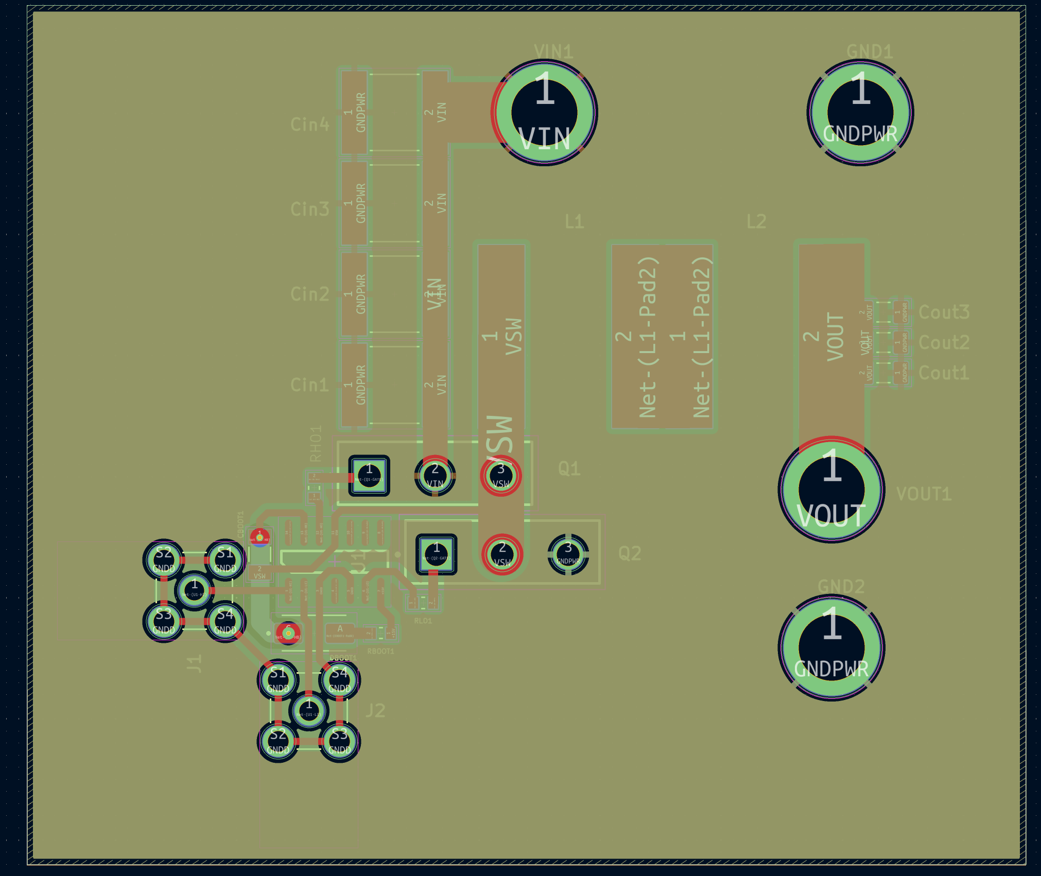
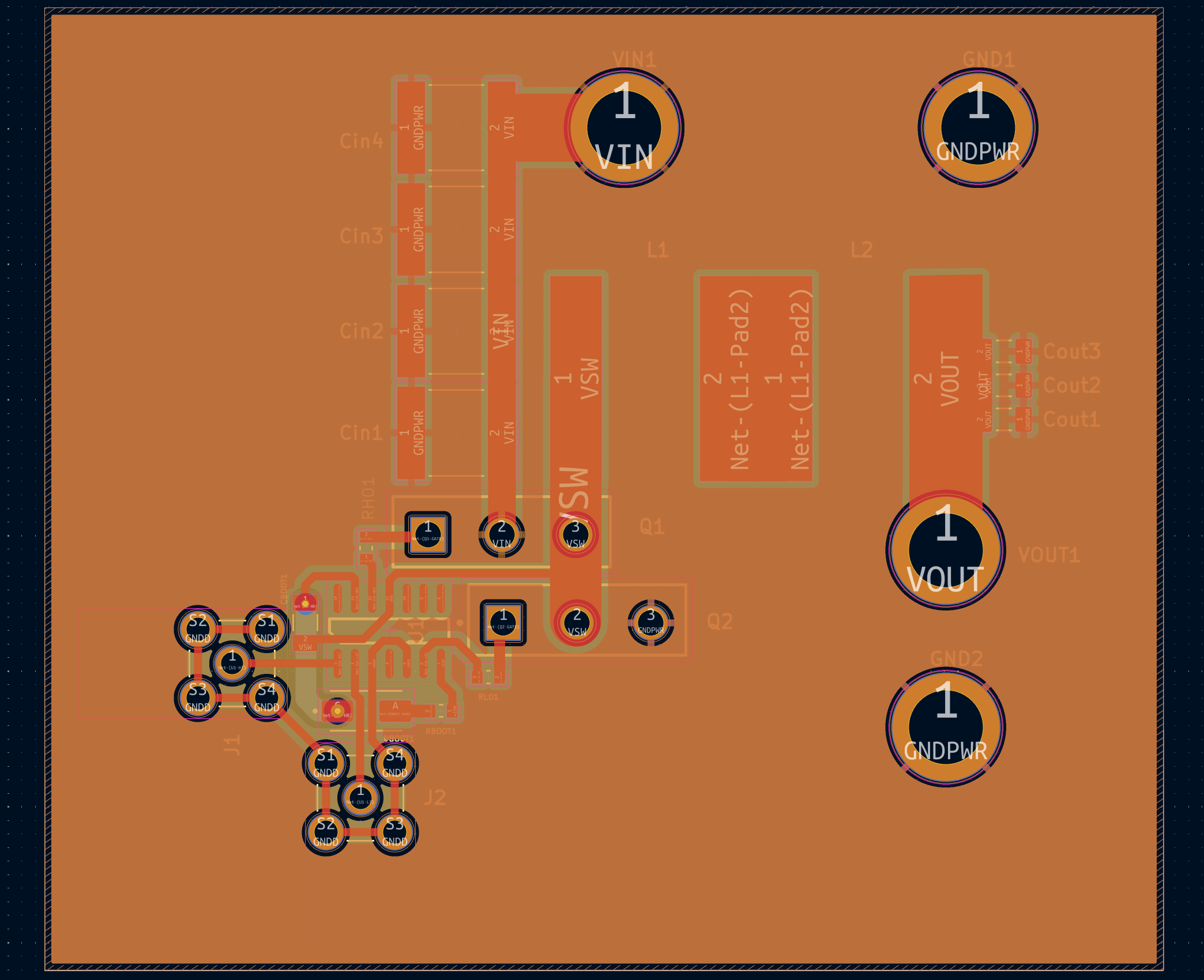
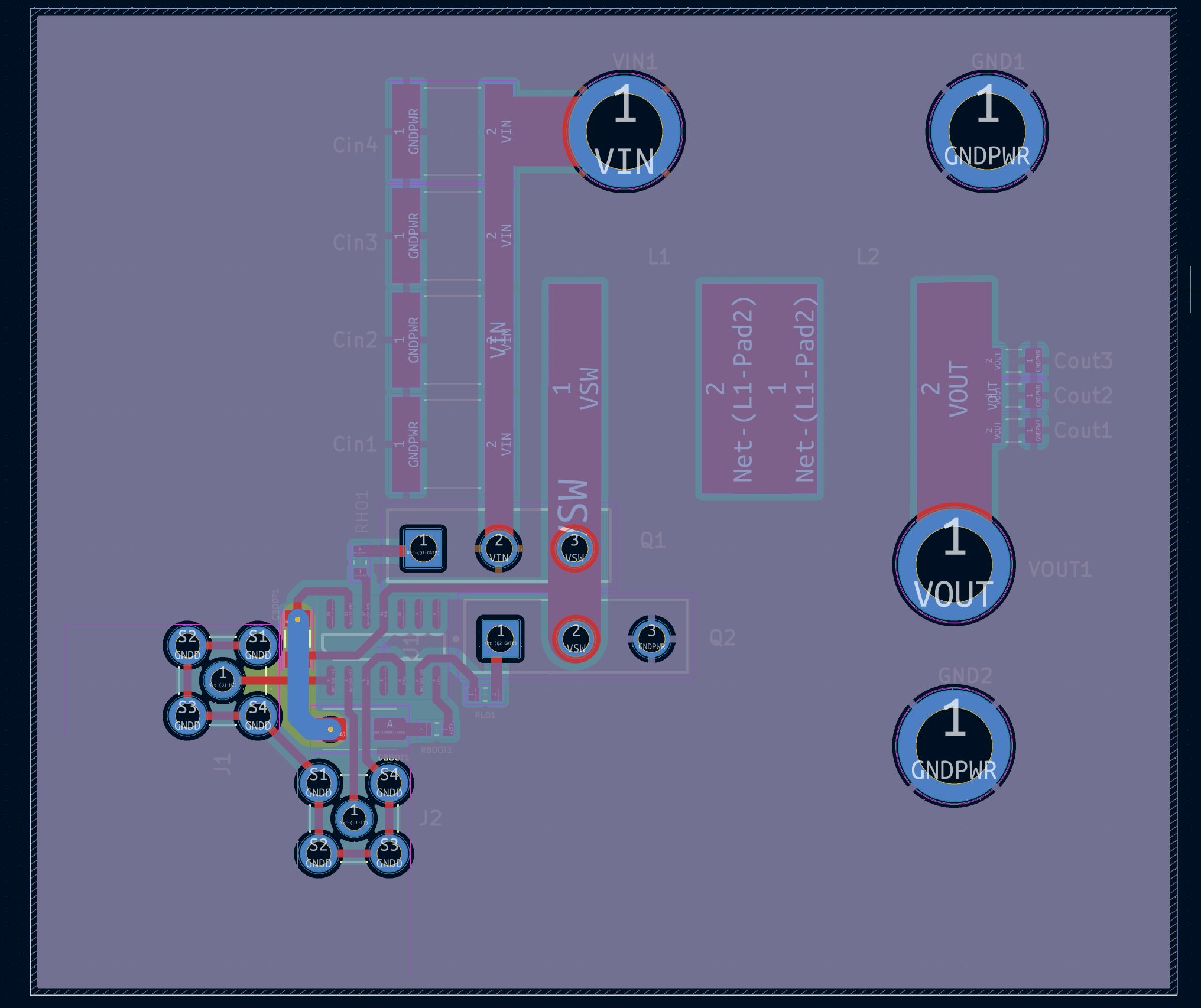
High-Voltage Buck Converter PCB Design (KiCad)
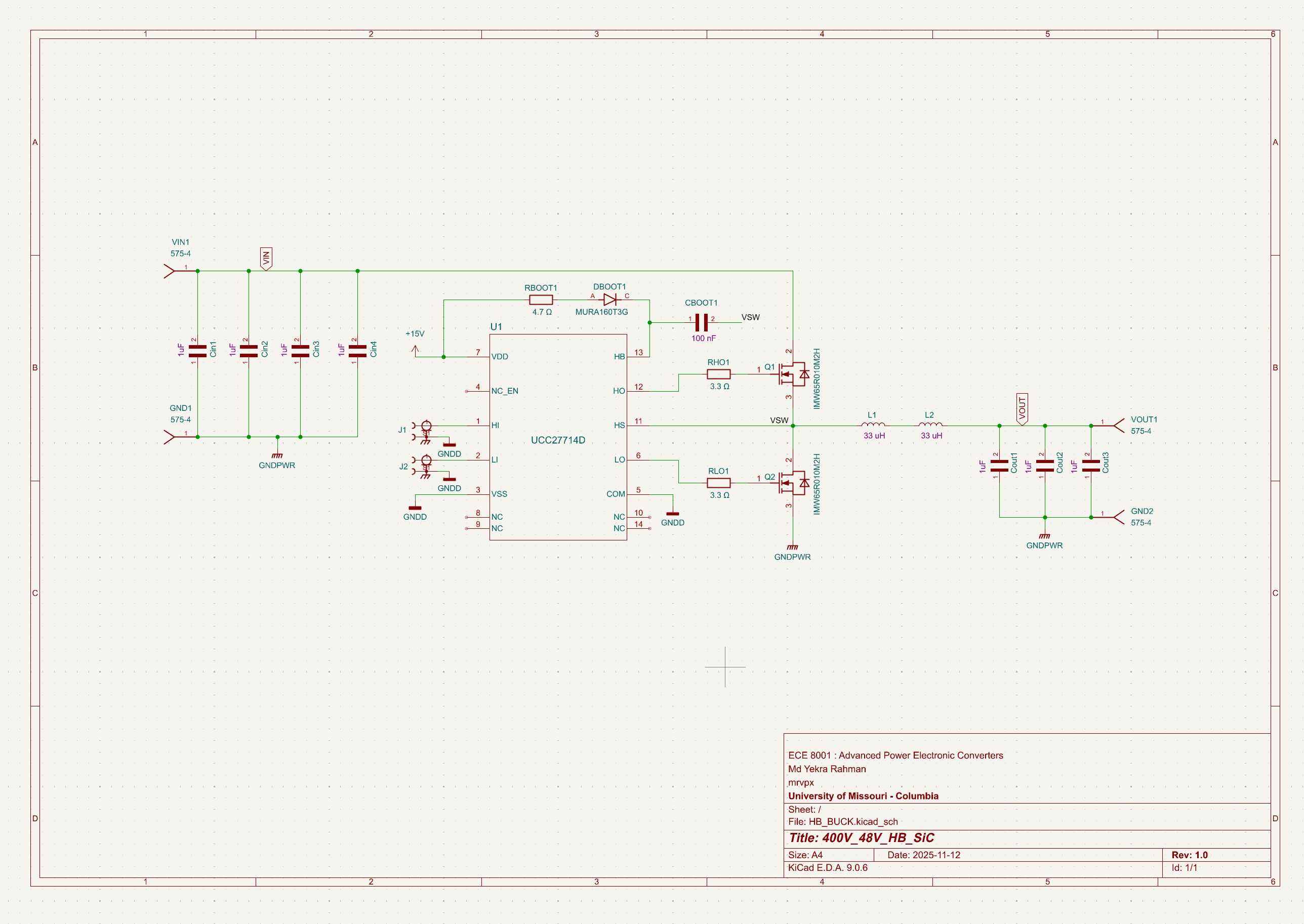
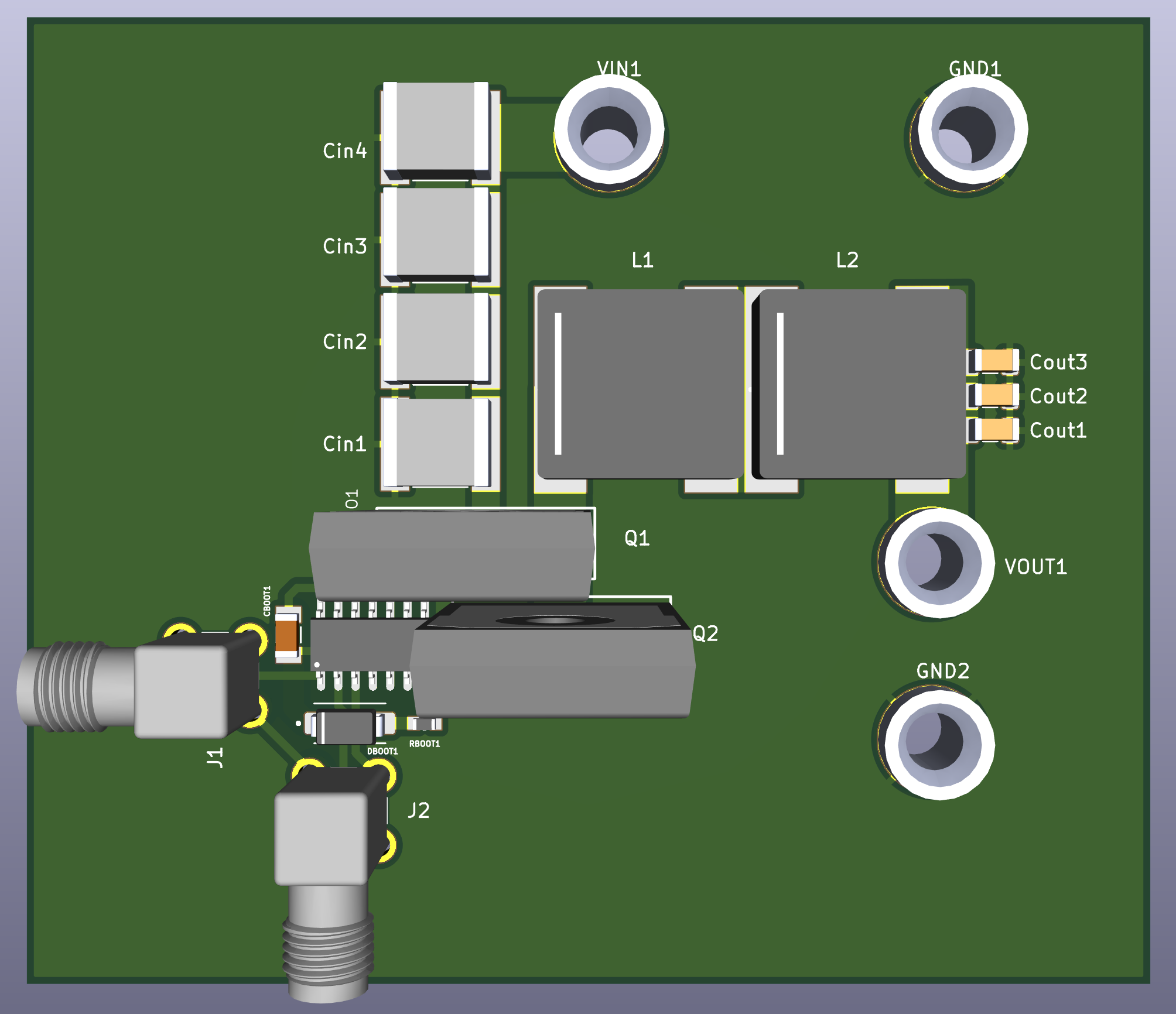
Complete schematic-to-layout workflow for a high-voltage synchronous buck converter, including custom footprint design, 4-layer PCB layout, and EMI-aware power routing using KiCad.
- Designed a synchronous half-bridge buck converter schematic in KiCad based on analytical CCM design calculations
- Selected and integrated 650 V SiC MOSFETs, high-side gate driver, bootstrap network, and passive components
- Manually created a custom PCB footprint for a non-standard SiC MOSFET package using datasheet dimensions
- Developed a complete 4-layer PCB stackup: Front (signals & switching), Inner GND, Inner POWER, and Back layer
- Applied EMI-aware layout practices to minimize high di/dt loop area and gate-drive parasitics
- Ensured tight gate-loop routing with individual gate resistors and close driver–MOSFET placement
- Implemented solid ground and power planes to reduce impedance, noise coupling, and voltage drop
- Validated mechanical clearances, footprint accuracy, and assembly feasibility using 3D PCB rendering
TCAD → Compact Modeling → Circuit-Level Validation
Physics-aware device modeling pipeline bridging TCAD simulations and real circuit behavior.
- Developed detailed TCAD device structures and physics setups for power and emerging WBG devices
- Generated DC, AC, and transient datasets tailored for compact model extraction
- Performed model calibration and consistency checks prior to circuit insertion
- Integrated extracted models into Spectre for converter and block-level verification
- Investigating switching behavior, parasitics, bias dependence, and numerical robustness
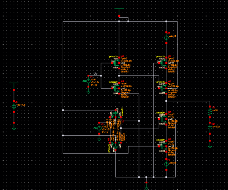
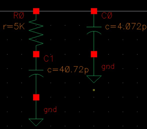
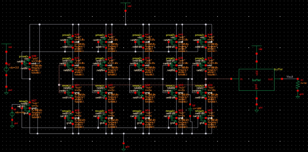
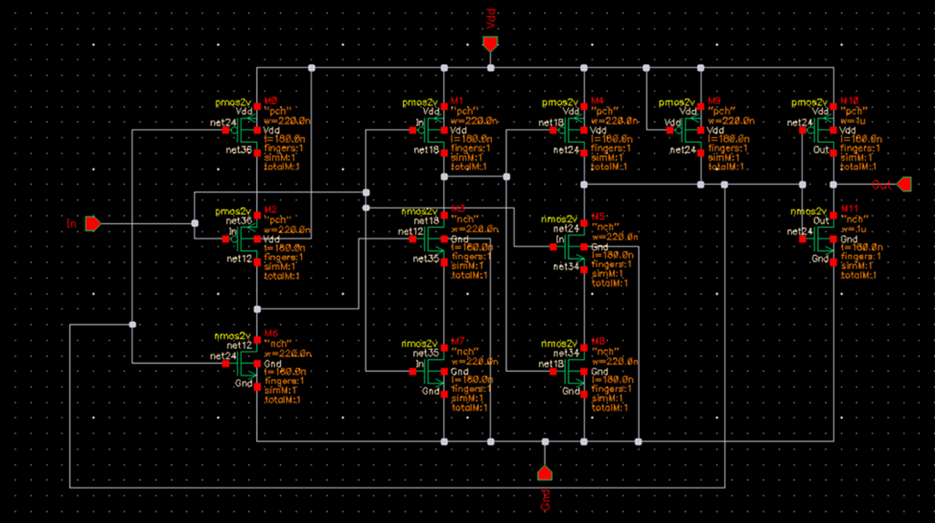
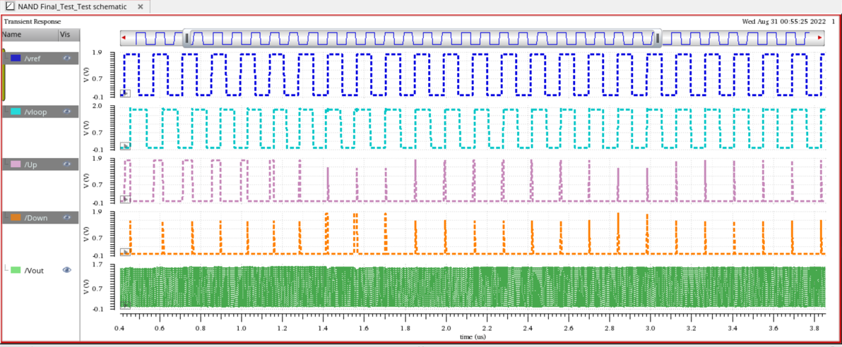
Phase-Locked Loop (PLL) — Transistor-Level Design
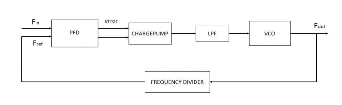
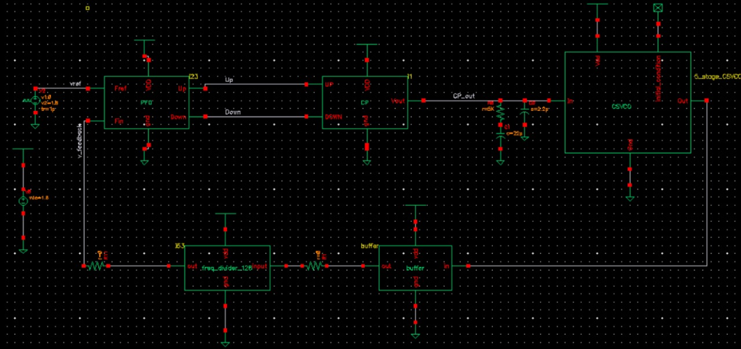
Fully custom phase-locked loop designed from scratch in Cadence Virtuoso, including PFD, charge pump, current-starved VCO, and frequency divider, validated through transient and steady-state simulations.
- Designed a complete PLL architecture using Cadence analog libraries with full transistor-level implementation
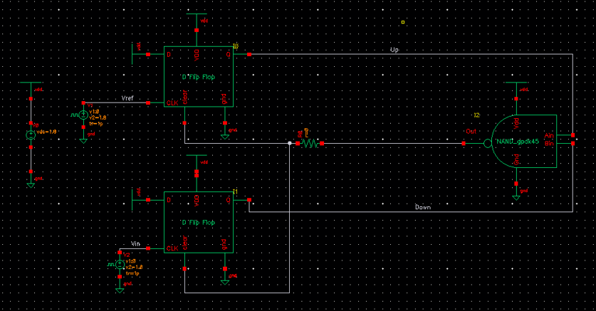
- Implemented a Phase Frequency Detector (PFD) with reset logic to eliminate dead-zone effects
- Designed a low-leakage charge pump ensuring matched up/down currents for minimal static phase error
- Developed a current-starved VCO with controllable oscillation frequency via control voltage tuning
- Integrated a frequency divider to enable frequency synthesis and feedback stabilization
- Validated lock acquisition, steady-state phase tracking, and frequency stability through transient simulations
- Analyzed loop behavior including tuning range, lock time, and control-voltage dynamics
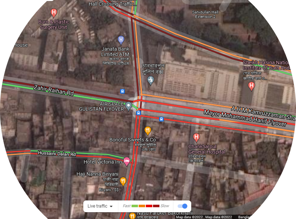
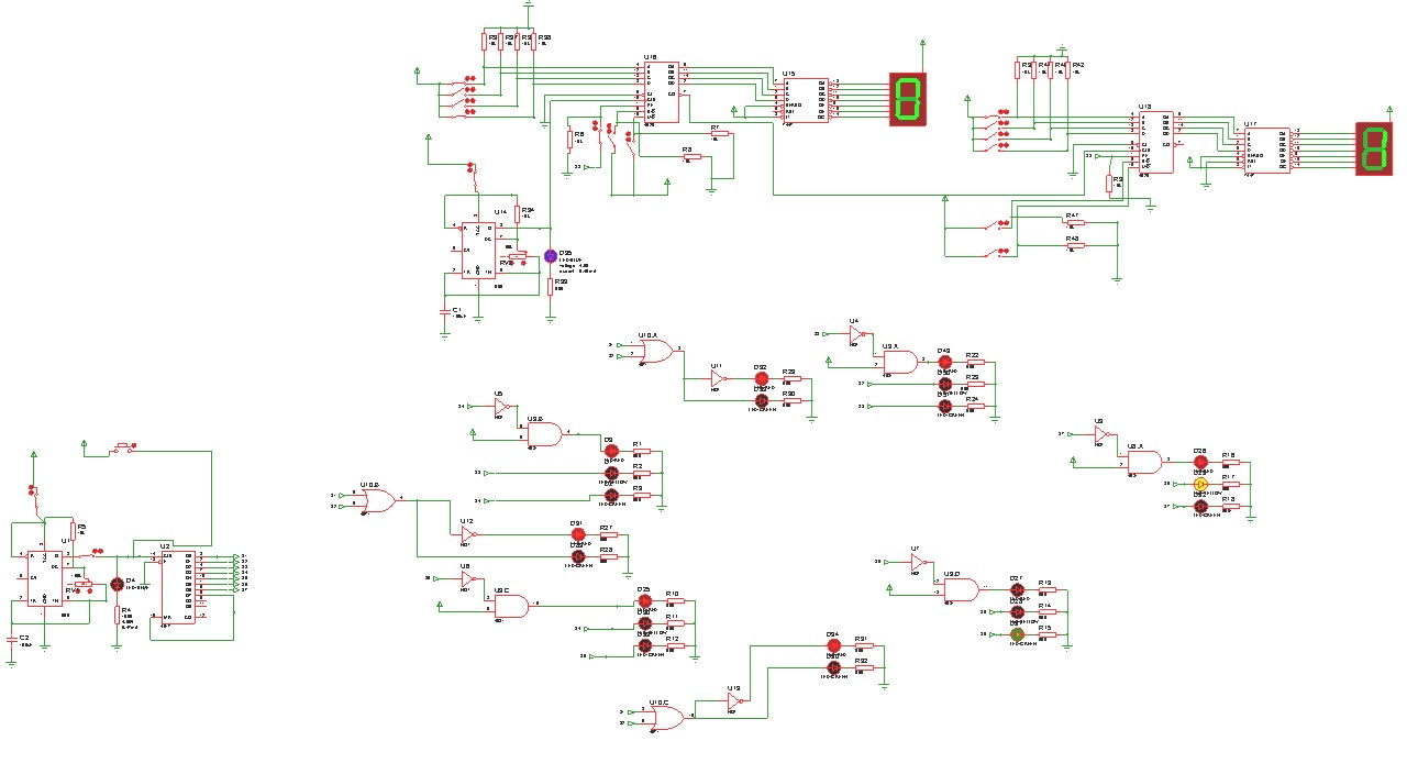
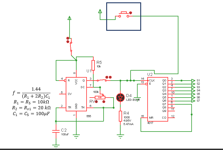
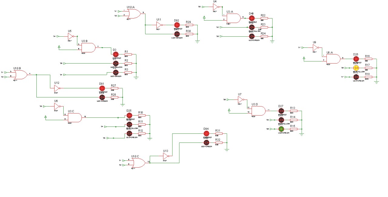
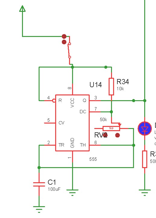
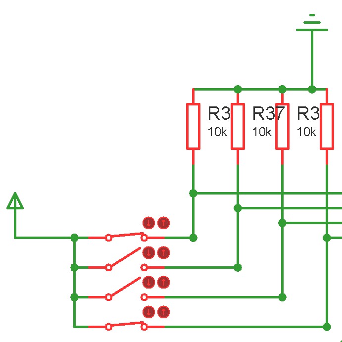
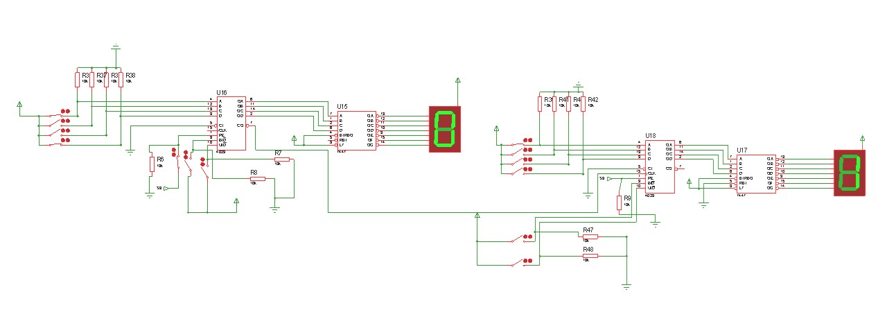
Automated Traffic Control System (Digital Logic Based)
Fully hardware-based automated traffic control system designed for a real-world five-road intersection (“Chankharpurl More”), implemented without microcontrollers or Arduino, using discrete logic ICs.
- Designed an automated traffic control system for a complex 5-way circular intersection
- Implemented complete control logic using digital ICs only, avoiding microprocessors and Arduino
- Developed timing and sequencing logic to manage safe traffic flow across all directions
- Simulated the full system behavior in Proteus to verify correctness and timing coordination
- Physically built and tested the system at hardware level using logic gates, counters, and timers
- Ensured proper signal transitions and fail-safe operation to prevent conflicting green signals
- Demonstrated a low-cost, reliable solution suitable for small urban intersections
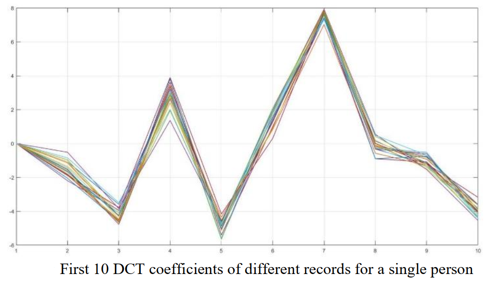
ECG-Based Biometric Recognition System
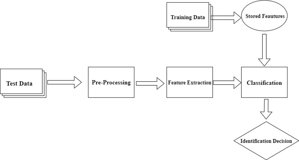
Signal-processing and machine-learning–based biometric authentication system using ECG signals, featuring robust preprocessing, feature extraction, and classification with cross-validation.
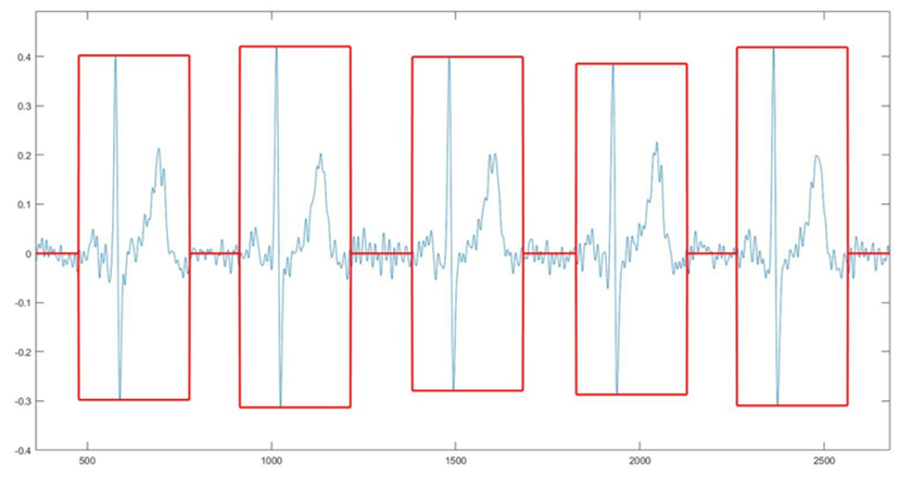
- Developed a biometric recognition system using electrocardiogram (ECG) signals as unique physiological identifiers
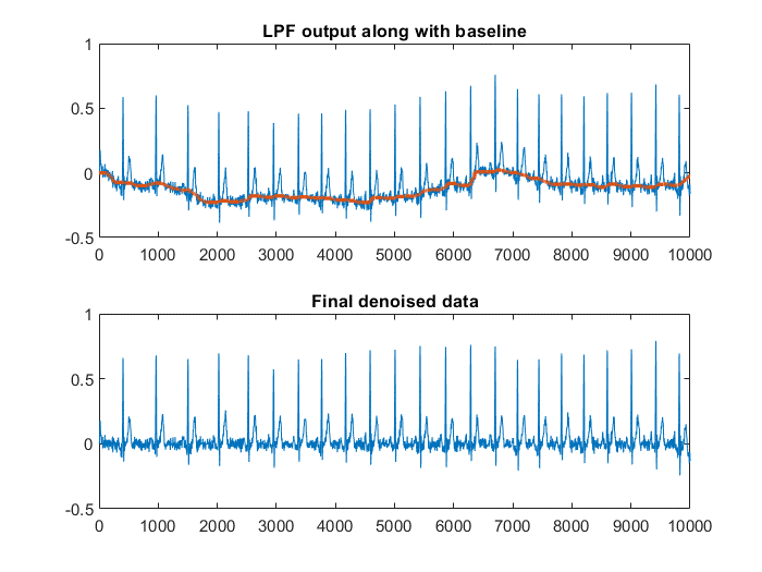
- Applied Chebyshev low-pass filtering and median filtering to remove noise and baseline wander
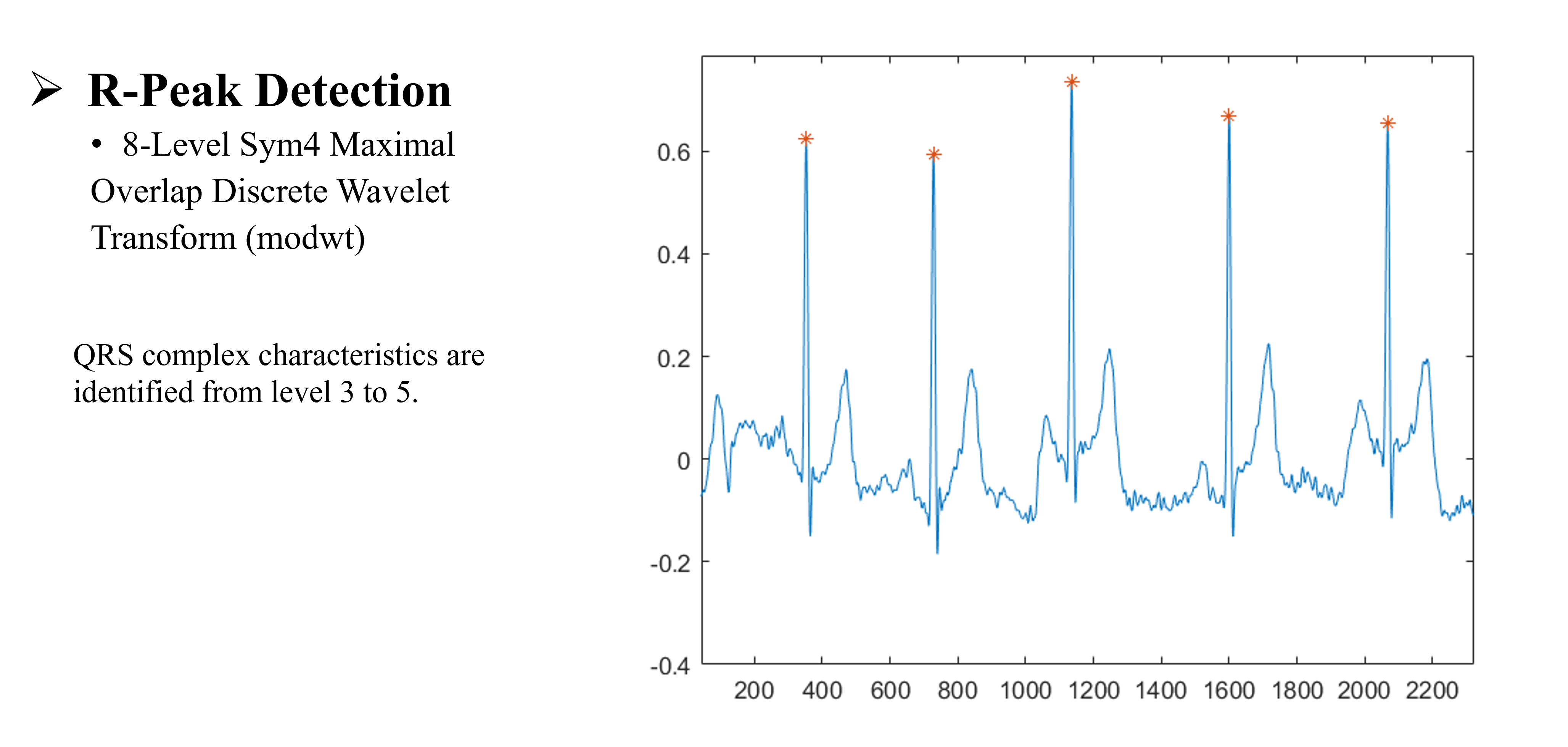
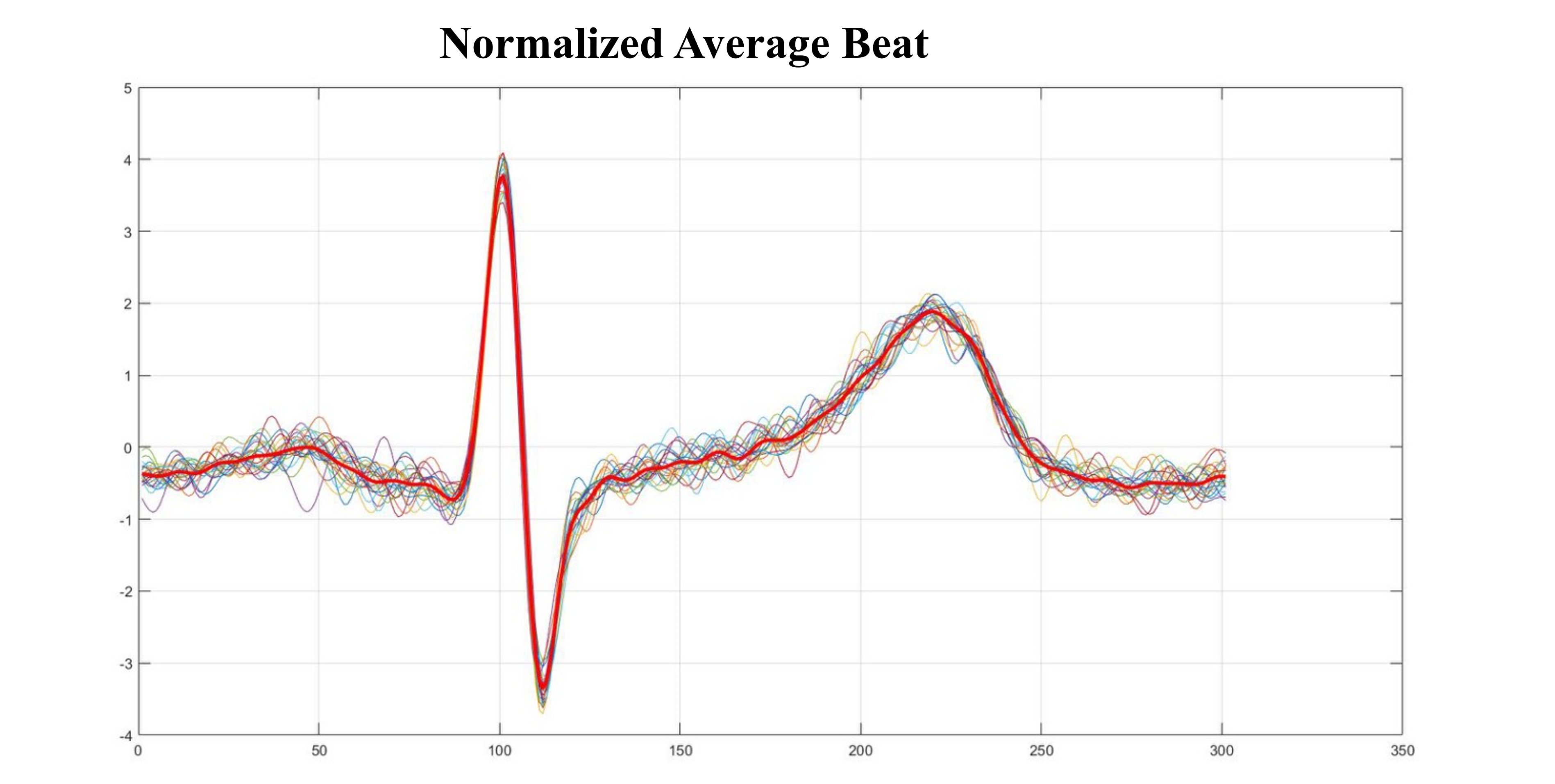
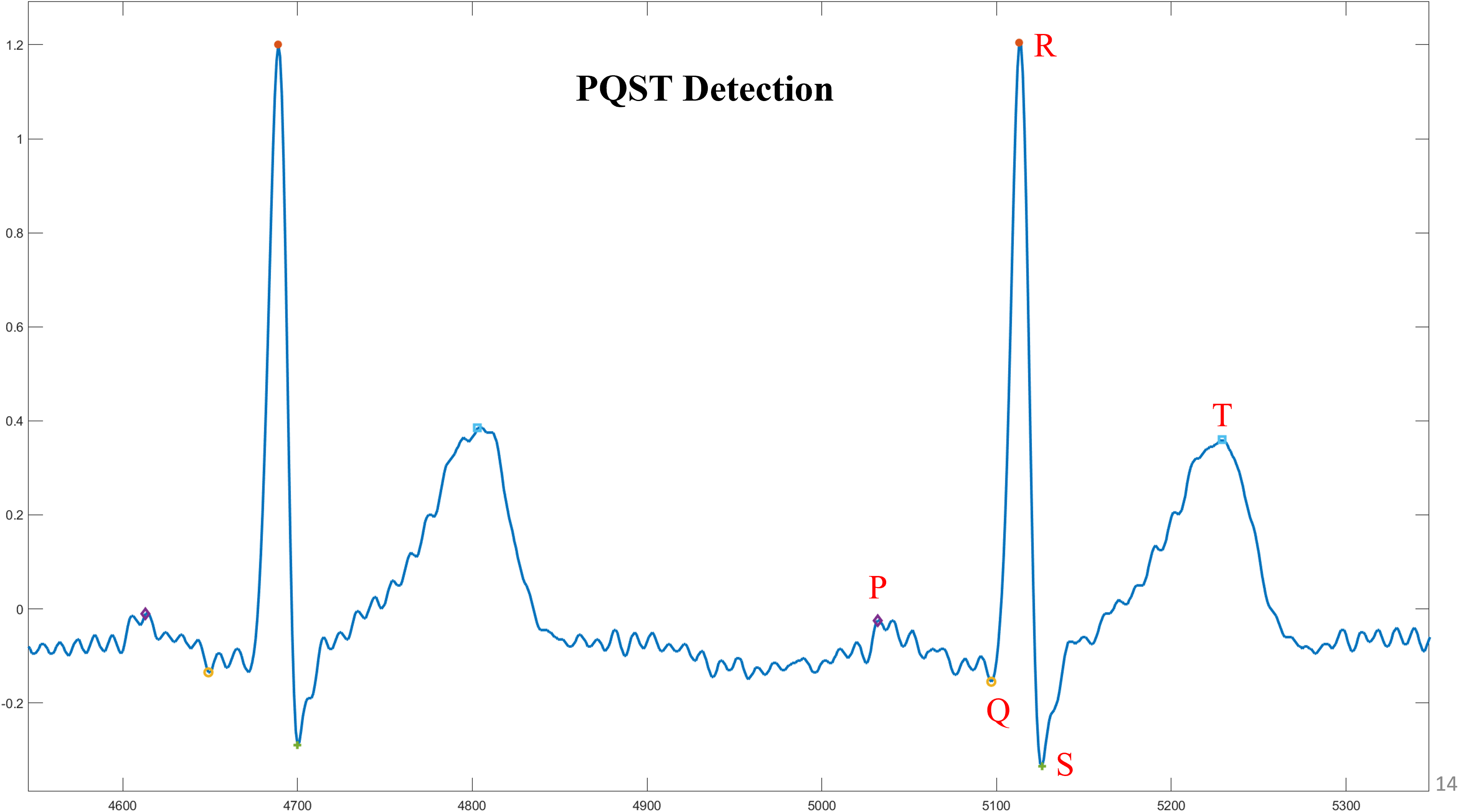
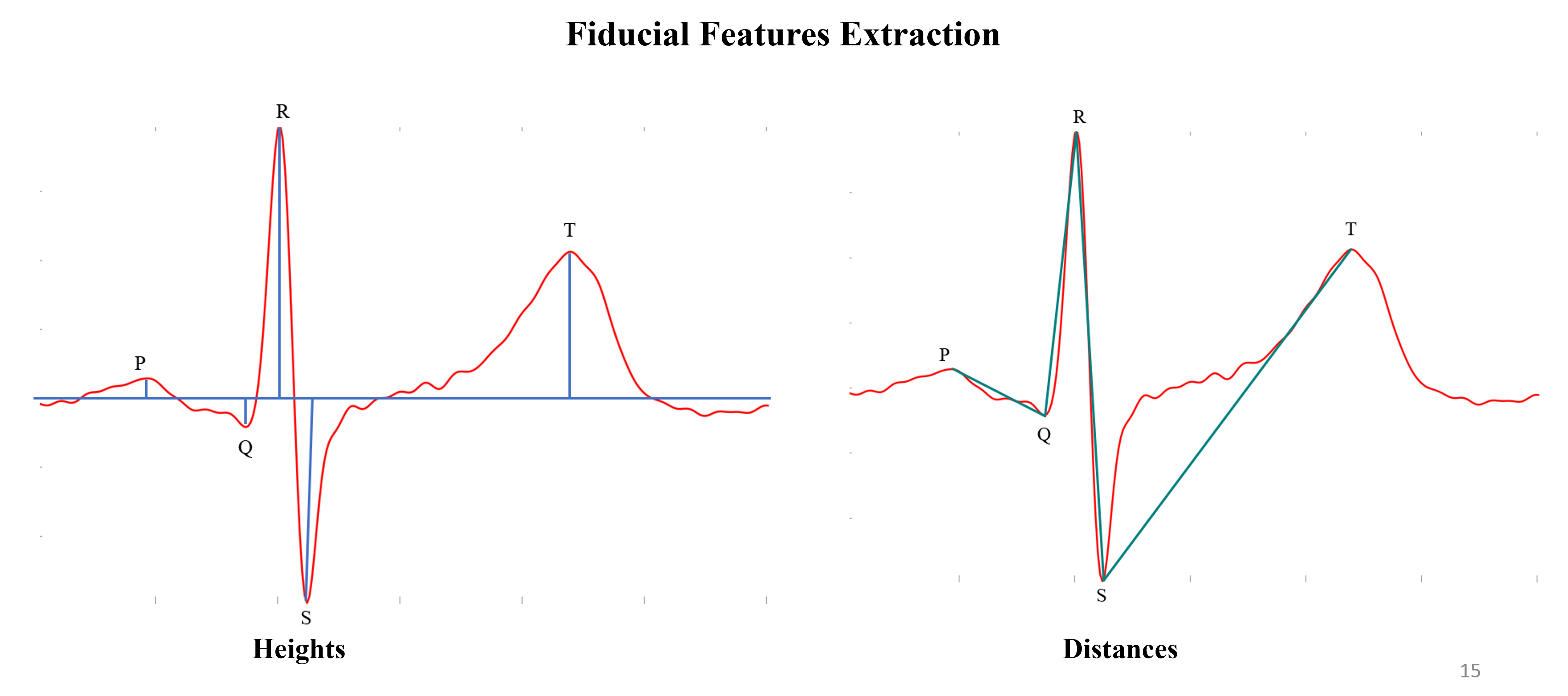
- Performed feature extraction using Maximal Overlap Discrete Wavelet Transform (MODWT)
- Designed a classification framework using Weighted K-Nearest Neighbors (WKNN) with Euclidean distance
- Evaluated system performance using 5-fold cross-validation to ensure robustness and generalization
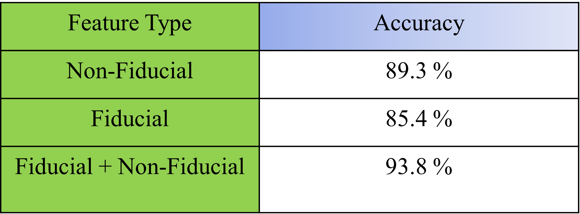
- Analyzed classification accuracy, sensitivity, and subject discrimination capability
- Demonstrated feasibility of ECG signals for secure, non-invasive biometric authentication
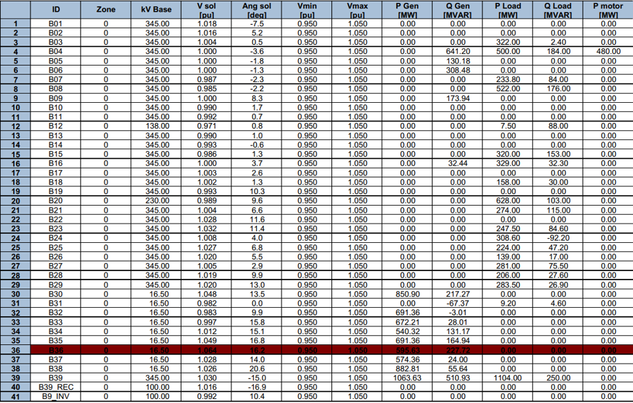
Impact of HVDC Connection & Large Industrial Loads on IEEE 39-Bus System
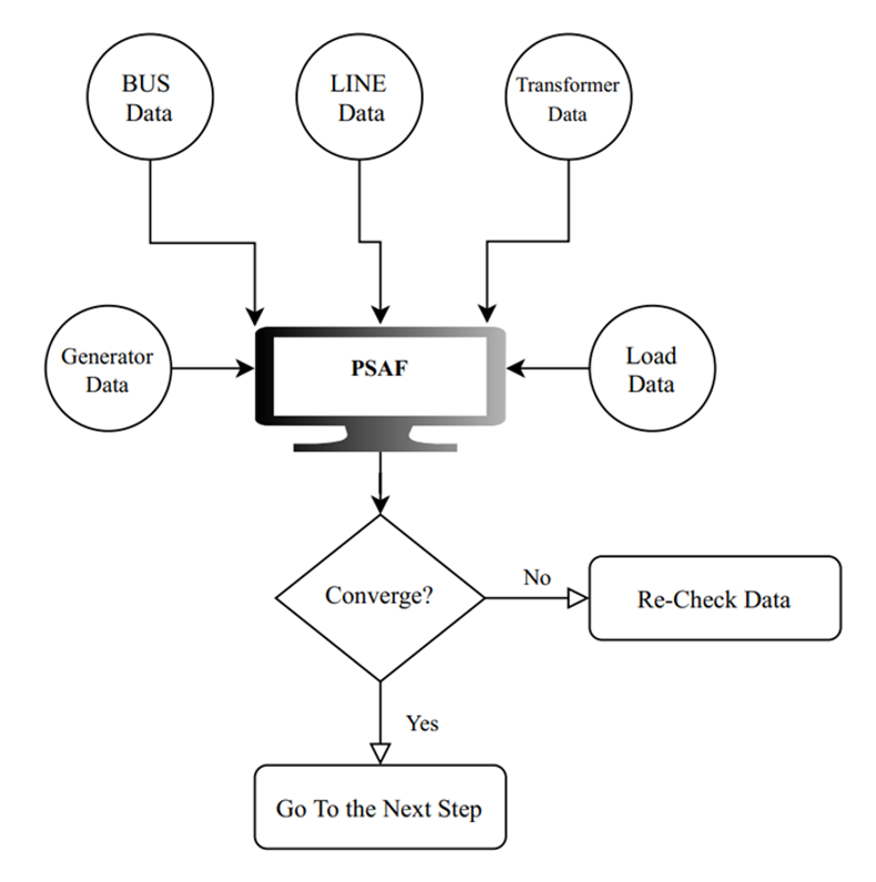
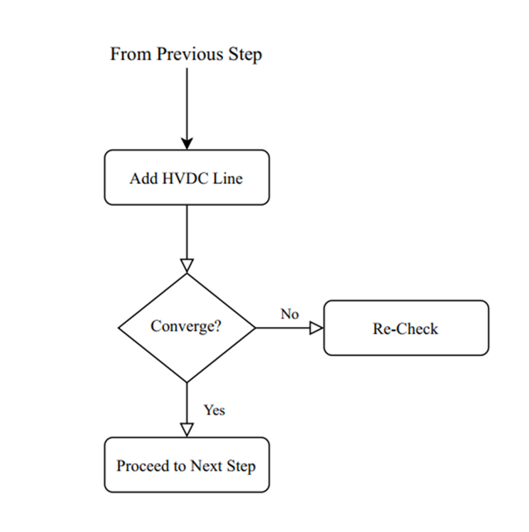
Power system stability and load-flow analysis of the IEEE 39-bus network, investigating voltage stability, line loading, and mitigation strategies under HVDC integration and large industrial loads using PSAF.
- Performed detailed load-flow analysis of the IEEE 39-bus power system using the Newton–Raphson method
- Modeled and integrated a point-to-point HVDC link between Bus-39 and Bus-9 to study system-level impacts
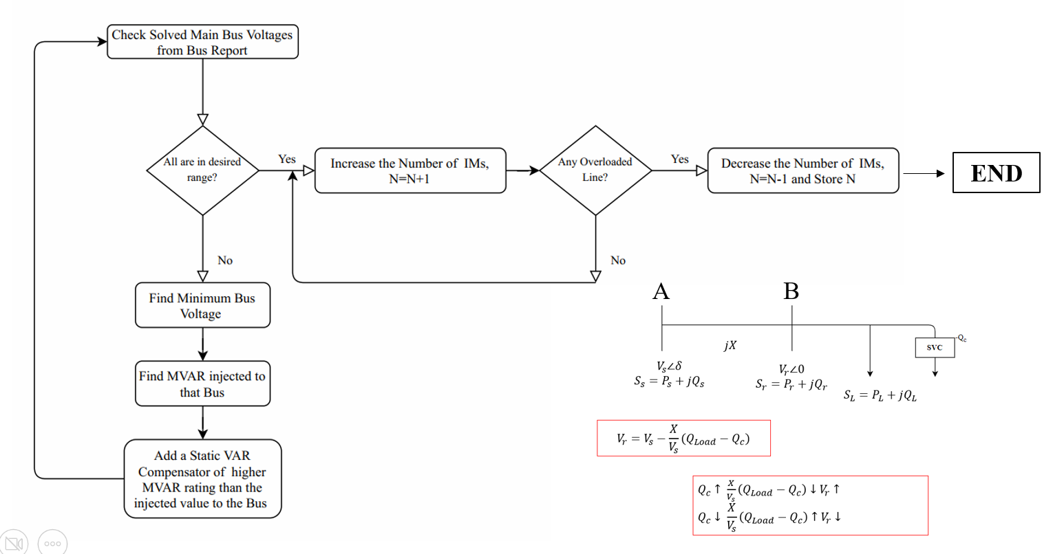
- Introduced large industrial loads modeled as induction motors to emulate real-world plant behavior
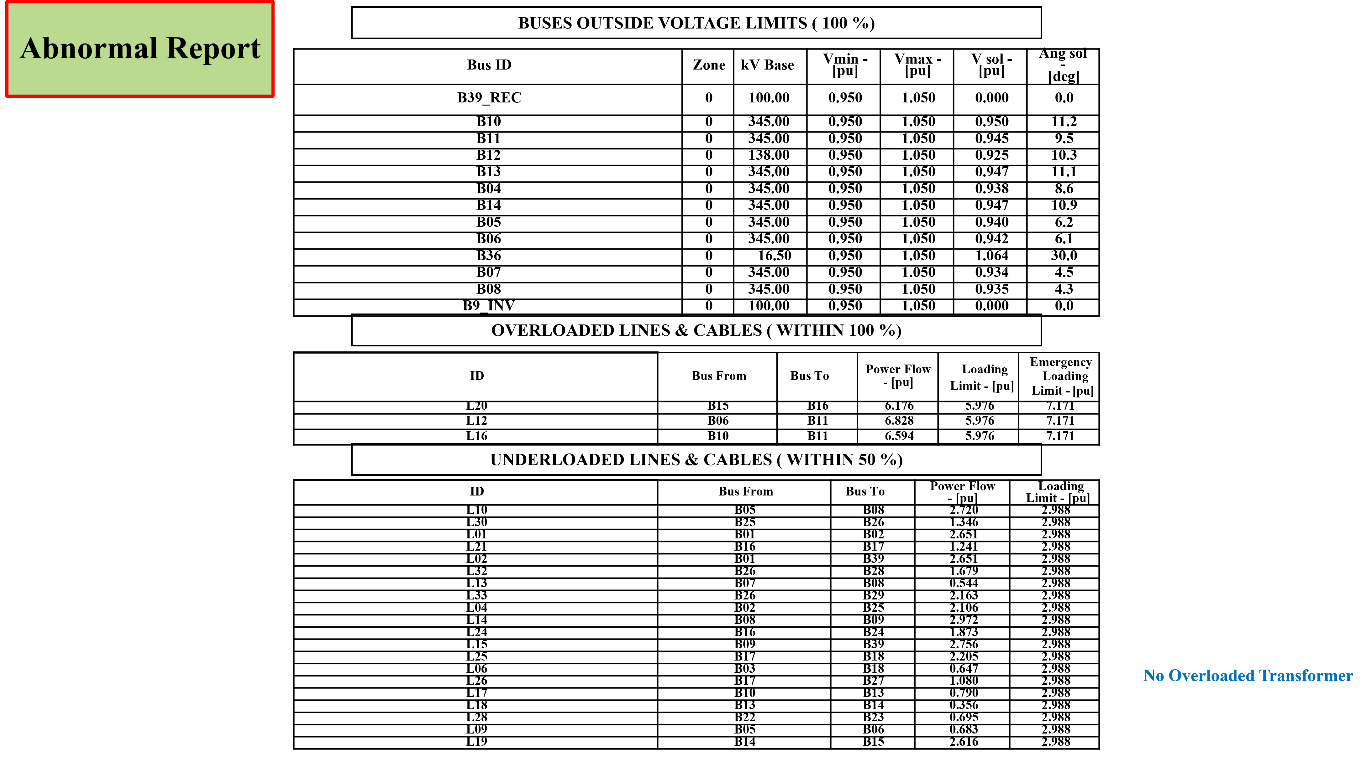
- Identified abnormal bus voltages, line overloads, and stability degradation due to heavy loading
- Designed and placed Static VAR Compensators (SVCs) to improve voltage regulation and system stability
- Compared pre- and post-mitigation bus reports to validate effectiveness of compensation strategies
- Demonstrated coordinated use of HVDC and reactive power support for robust grid operation


Publications
Journal Papers
Loading.